- 您现在的位置:买卖IC网 > Sheet目录488 > NTD95N02RT4G (ON Semiconductor)MOSFET N-CH 24V 12A DPAK
�� �
�
�NTD95N02R�
�Power� MOSFET�
�95� Amps,� 24� Volts�
�N?Channel� DPAK�
�Features�
�?� High� Power� and� Current� Handling� Capability�
�?� Fast� Switching� Performance�
�?� Low� R� DS(on)� to� Minimize� Conduction� Loss�
�?� Low� Gate� Charge� to� Minimize� Switching� Losses�
�?� Pb?Free� Packages� are� Available�
�http://onsemi.com�
�V� (BR)DSS� R� DS(ON)� TYP� I� D� MAX*�
�4.5� m� W� @� 10� V�
�24� V� 95� A�
�5.9� m� W� @� 4.5� V�
�*I� D� MAX� in� the� product� summary� table� is� continuous�
�and� steady� at� 25� °� C.�
�Applications�
�?� CPU� Motherboard� Vcore� Applications�
�?� High� Frequency� DC?DC� Converters�
�?� Motor� Drives�
�?� Bridge� Circuits�
�MAXIMUM� RATINGS� (T� J� =� 25� °� C� unless� otherwise� specified)�
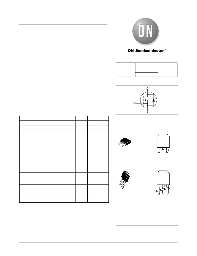
�G�
�D�
�S�
�Parameter�
�Drain?to?Source� Voltage�
�Gate?to?Source� Voltage�
�Symbol�
�V� DSS�
�V� GS�
�Value�
�24�
�±� 20�
�Unit�
�V�
�V�
�MARKING� DIAGRAMS�
�&� PIN� ASSIGNMENTS�
�4�
�Thermal� Resistance,� Junction?to?Case�
�Total� Power� Dissipation� @� T� A� =� 25� °� C�
�Drain� Current� –�
�?� Continuous� @� T� A� =� 25� °� C,� Limited� by� Package�
�?� Continuous� @� T� A� =� 25� °� C,� Limited� by� Wires�
�Thermal� Resistance,� Junction?to?� Ambient�
�(Note� 1)�
�?� Total� Power� Dissipation� @� T� A� =� 25� °� C�
�?� Drain� Current� ?� Continuous� @� T� A� =� 25� °� C�
�R� q� JC�
�P� D�
�I� D�
�I� D�
�R� q� JA�
�P� D�
�I� D�
�1.45�
�86�
�95�
�32�
�52�
�2.4�
�15.8�
�°� C/W�
�W�
�A�
�A�
�°� C/W�
�W�
�A�
�1� 2�
�3�
�4�
�DPAK�
�CASE� 369AA�
�(Surface� Mount)�
�STYLE� 2�
�1�
�Gate�
�Drain�
�2�
�Drain�
�3�
�Source�
�Thermal� Resistance,� Junction?to?Ambient�
�(Note� 2)�
�?� Total� Power� Dissipation� @� T� A� =� 25� °� C�
�?� Drain� Current� ?� Continuous� @� T� A� =� 25� °� C�
�Operating� Junction� and� Storage� Temperature�
�Continuous� Source� Current� (Body� Diode)�
�R� q� JA�
�P� D�
�I� D�
�T� J� ,�
�T� STG�
�I� S�
�100�
�1.25�
�12�
�?55� to�
�150�
�45�
�°� C/W�
�W�
�A�
�°� C�
�A�
�4�
�DPAK�
�CASE� 369D�
�(Straight� Lead)�
�4�
�Drain�
�Single� Pulse� Drain?to?Source� Avalanche�
�Energy� –� (V� DD� =� 25� V,� V� G� =� 10,� I� PK� =� 13� A,�
�L� =� 1� mH,� R� G� =� 25� W� )�
�E� AS�
�84�
�mJ�
�1�
�2�
�3�
�STYLE� 2�
�Lead� Temperature� for� Soldering� Purposes�
�(1/8� in� from� case� for� 10� seconds)�
�T� L�
�260�
�°� C�
�1� 2� 3�
�Gate� Drain� Source�
�Stresses� exceeding� Maximum� Ratings� may� damage� the� device.� Maximum�
�Ratings� are� stress� ratings� only.� Functional� operation� above� the� Recommended�
�Operating� Conditions� is� not� implied.� Extended� exposure� to� stresses� above� the�
�Recommended� Operating� Conditions� may� affect� device� reliability.�
�1.� Surface� mounted� on� FR4� board� using� 1� in� sq� pad� size� (Cu� area� =� 1.127� in� sq�
�[1� oz]� including� traces).�
�Y�
�WW�
�T95N02R�
�G�
�=� Year�
�=� Work� Week�
�=� Device� Code�
�=� Pb?Free� Package�
�2.� Surface� mounted� on� FR4� board� using� the� minimum� recommended� pad� size�
�(Cu� area� =� 0.412� in� sq).�
�ORDERING� INFORMATION�
�See� detailed� ordering� and� shipping� information� in� the� package�
�dimensions� section� on� page� 4� of� this� data� sheet.�
�?� Semiconductor� Components� Industries,� LLC,� 2006�
�July,� 2006� ?� Rev.� 3�
�1�
�Publication� Order� Number:�
�NTD95N02R/D�
�发布紧急采购,3分钟左右您将得到回复。
相关PDF资料
NTDV18N06LT4G
MOSFET N-CH 60V 18A DPAK
NTDV20N06T4G
MOSFET N-CH 60V 20A DPAK
NTDV3055L104-1G
MOSFET N-CH 60V 12A IPAK
NTDV5804NT4G
MOSFET N-CH 40V 69A DPAK
NTF3055-100T3LF
MOSFET N-CH 60V 3A SOT223
NTF3055-160T1
MOSFET N-CH 60V 2A SOT223
NTF3055L108T3LFG
MOSFET N-CH 60V 3A SOT223
NTF3055L175T1
MOSFET N-CH 60V 2A SOT223
相关代理商/技术参数
NTD985
制造商:未知厂家 制造商全称:未知厂家 功能描述:TRANSISTOR | BJT | DARLINGTON | NPN | 60V V(BR)CEO | 2A I(C) | TO-126VAR
NTD986
制造商:未知厂家 制造商全称:未知厂家 功能描述:TRANSISTOR | BJT | DARLINGTON | NPN | 80V V(BR)CEO | 2A I(C) | TO-126VAR
NTD987
制造商:未知厂家 制造商全称:未知厂家 功能描述:TRANSISTOR | BJT | DARLINGTON | NPN | 400V V(BR)CEO | 5A I(C) | TO-220AB
NTDP3-90PT82
制造商:ITT Interconnect Solutions 功能描述:NTDP3-90PT82 - Bulk
NTDRT21
制造商:OMRON AUTOMATION AND SAFETY 功能描述:DEVICENET COM MODULE NT31/631 制造商:Omron Electronic Components LLC 功能描述:Programmable Terminal Devicenet Interface Unit
NT-DRT21
功能描述:LCD 触摸面板 DEVICENET COM M ODULE NT31/631
RoHS:否 制造商:3M Touch Systems 类型:P-MVA 大小:22 in 绝缘电阻: 封装:Bulk
NTDV18N06LT4G
功能描述:MOSFET NFET DPAK 60V 18A RoHS:否 制造商:STMicroelectronics 晶体管极性:N-Channel 汲极/源极击穿电压:650 V 闸/源击穿电压:25 V 漏极连续电流:130 A 电阻汲极/源极 RDS(导通):0.014 Ohms 配置:Single 最大工作温度: 安装风格:Through Hole 封装 / 箱体:Max247 封装:Tube
NTDV20N06LT4G
功能描述:MOSFET NFET 60V 20A 48MOHM RoHS:否 制造商:STMicroelectronics 晶体管极性:N-Channel 汲极/源极击穿电压:650 V 闸/源击穿电压:25 V 漏极连续电流:130 A 电阻汲极/源极 RDS(导通):0.014 Ohms 配置:Single 最大工作温度: 安装风格:Through Hole 封装 / 箱体:Max247 封装:Tube